Quickturn Design Systems, Inc.
55 West Trimble Rd.
San Jose, CA 95131-1013
(408) 914-6000
This paper was originally published in the Design Automation Conference Proceedings (DAC), June 1998, pgs. 668-671
Permission to make digital/hard copy of all or part of this work for personal or classroom use is granted without fee provided that copies are not made or distributed for profit or commercial advantage, the copyright notice, the title of the publication and its date appear, and notice is given that copying is by permission of ACM, Inc. To copy otherwise, to republish, to post on servers or to redistribute to lists, requires prior specific permission and/or a fee.
Included here by permission of the ACM.
As the density of VLSI circuits increases, software techniques cannot effectively simulate designs through the millions of simulation cycles needed for verification. Emulation can supply the necessary capacity and performance, but emulation is limited to designs that are structural or can be synthesized. This paper discusses a new system architecture that dramatically accelerates event-driven behavioral simulation and describes how it is merged with emulation.
reconfigurable computing, event-driven simulation
As ASIC design complexity has increased, logic simulation has evolved. Early simulators compiled designs, written in Verilog or VHDL hardware description languages (HDL), into a pseudo-instruction set for interpretation by a software "machine". To improve performance, many simulators now compile HDL designs directly into a microprocessor instruction set (e.g., SPARC, HP PA-RISC, powerPC) [12]. These compiled simulators can be more than ten times the speed of interpreted simulators. The performance improvement yielded by compiled simulation is limited by the overhead of event processing. Cycle-based simulators take advantage of native code performance, but avoid event processing overhead by only simulating synchronous designs in structural or synthesizable form.
Although the performance of software simulators has constantly improved, the rate of improvement falls far short of the rate at which design density is increasing. Hardware acceleration, usually based on a network of custom processors, has been used to increase the speed and capacity of simulation by up to 100 times. Hardware emulation, where the hardware design is emulated on a large network of programmable logic (FPGAs) [14], has been used to increase simulation speed and capacity by up to 10,000 times [11].
Emulation sacrifices generality for performance; it cannot be used to simulate behavioral circuit models that contain delays or other constructs that are either non-structural or cannot be synthesized [2] into gate-level circuitry. The high speed of emulation also introduces its own constraints. To supply data (test vectors or other system input) at a rate that matches emulation performance, existing emulation systems must be used "in-circuit" with the target system hardware.
Both hardware accelerators and emulators have been combined with software simulators, which can be used to simulate the behavioral component of a design. Communication between the software simulator and the emulated design usually takes place over Ethernet or across a system bus, like VME. This approach has drawbacks:
Reconfigurable computing systems using field programmable gate arrays (FPGAs) have been proposed by a number of research groups [3, 9]. Several research groups have coupled reconfigurable logic with processors [4, 9, 13]. The HARP system [9] couples FPGAs with a 32-bit transputer microprocessor [7]. The Garp processor [13], proposed by the BRASS research group at UC Berkeley, is a custom VLSI design that couples a MIPS II core with an on-chip FPGA array. However, the application of these techniques to event-driven simulation has not been adequately explored.
This paper describes a reconfigurable computing system that has been applied to the event driven simulaton of large VLSI circuit designs. The foundation for this reconfigurable computing system is an FPGA-based emulator, which provides large blocks of reconfigurable logic. The system hardware is supported by a compiler that can compile a behavioral Verilog HDL description of the design. This system has a number of advantages:
The reconfigurable computer system is pictured in Figure 1, below. The system consists of one or more emulation modules. Each emulation module consists of:
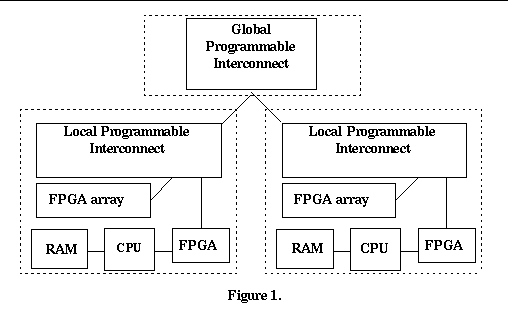
The FPGA array in each emulation module is interconnected to all of the other emulation module FPGA arrays via a programmable interconnect. The programmable interconnect allows all FPGA arrays to be treated as if they were a single large FPGA array. Each emulation module runs a simple real time operating system to manage behavioral simulation and logic netlist emulation. A control processor (not shown) supports higher level operating system functions such as TCP/IP network access, disk, and the network file system (NFS).
To the user, the reconfigurable computer system appears to be a simulation server on the local area network. However, only one simulation may run on the system at any given time.
Compiling a behavioral Verilog design can be logically divided into two tasks: compiling behavioral Verilog into assembly language and synthesizing a netlist to program the FPGA array.
The Verilog [6] compiler serves as the front end for this process. The Verilog compiler scans and parses the input and produces an abstract syntax tree intermediate in memory. The module hierarchy is expanded; parameters, "defparams", and hierarchical names are resolved. Semantic analysis is then performed and functions are in-lined. A transformation pass does tree-to-tree translation to produce an intermediate form that can be more easily broken up into schedulable processes. Later passes compile the processes into control flow graphs and into powerPC [5] assembly instructions.
Each schedulable process created by the Verilog compiler has a set of data inputs and outputs. The partitioning and netlist creation software treats the processes as design units (e.g., module instances) and enters them into a design unit database. The purely structural parts of a Verilog design skip many of these steps.
Event detection and scheduling logic is synthesized from the behavioral design. Verilog variables that are arguments to module instances or triggers for events are synthesized into latches in the FPGA array. Other variables are allocated in processor memory. Each variable allocated in hardware is addressed with a unique hardware tag.
The partitioning of variables between FPGA hardware and processor memory is illustrated by module sum, (see Figure 2), below. In this module, the variables reset and clk are event triggers and the variable sum is a module output. Since these variables are involved either with events or module interconnection, they are allocated in the FPGA hardware. The local variable val is not a trigger or a module argument, so it is allocated in the processor memory.
module sum( reset, clk, sum );
input reset, clk;
output [7:0] sum;
reg [3:0] val;
reg [7:0] sum;


  always @(posedge clk)
  begin
    sum = sum + val;
    val = val + 1;
  end

  always @(posedge reset)
  begin
    sum = 0;
    val = 1;
  end

endmodule
Each process created by the Verilog compiler consists of a block of code and a set of triggering conditions: for example @(a or b) or #4. While translating the Verilog design, the Verilog compiler passes information to the hardware mapping phase. Structural module definitions are ultimately mapped directly into gate equivalents in the FPGA arrays. For behavioral processes, the hardware mapping phase takes the Verilog compiler's definition for a process and creates a data base element for it. This consists of three parts: an interface specification (data inputs and outputs), the triggering conditions, and a pointer to the code for the process.
The process interface specification is compiled into a set of addressable registers in the FPGA array . Each triggering condition is synthesized into its hardware equivalent. When a process is instantiated, its synthesized triggering condition circuitry is instantiated along with it. The triggering condition is a boolean expression with additional operators:
Edge operators are implemented as hardware edge detectors. Delay is implemented as a down counter preset to the delay value at the positive edge of its input signal.
A simulation cycle is divided into four subcycles: active, inactive, non-blocking, and monitor. Each triggering condition is assigned to one of these subcycles. This information is retained for use in event queue generation.
A process may refer to variables allocated as registers in the FPGA array or in processor memory (RAM). A two-step process effects the transfer of variable information between the processor and the FPGA array:
When all structural and process module instantiations are complete, a partitioning algorithm is run. This divides the design into sections, each of which will fit onto an emulation module (see Figure 1). The partitioning algorithm also defines the connections between the emulation modules. After the process components and structural components are placed into the emulation modules, a levelization algorithm provides a static prioritization which is used to generate the event queue. The synthesized logic for each triggering condition is connected to the associated event circuitry. Each separate event circuit in the event queue is given a unique identifier or tag. A software table, created by the code generation phase of the Verilog compiler, maps each process tag to a pointer to the start of the associated process. Each emulation module executable (consisting of one or more processes) is linked with a "main" section that contains a dispatch loop that waits for a hardware event tag. When the software dispatch loop reads the process tag from the tag register, it fetches the process address and branches to the start of the process.
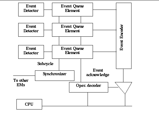
Figure 3 diagrams the event queue mechanism. The block labeled "Event Encoder" is synthesized as part of hardware compilation. The event encoder generates the process tags that identify processes to be executed in response to hardware events. When a triggering condition is met, the event detector associated with the synthesized triggering logic "fires". Subject to inhibition by the synchronizer, the asserted event captured by the event queue element presents its associated software tag to be read by the software dispatch loop. After the dispatch loop reads and acknowledges the tag, the event queue prepares the next process tag, if any other events are asserted. When the process invoked by the dispatch loop completes, control returns to the dispatch loop and another tag is read. When all processors have exhausted their event queues for a particular simulation cycle, the synchronizer re-starts the hardware simulation clock. Hardware clocking again proceeds until an event is triggered.
The synchronizer in Figure 3 serves two related purposes:
When an event is active on any processor, the hardware clock is halted until the event is serviced. This maintains simulation-clock and subcycle synchrony across all emulation modules -- in essence, simulation time proceeds only when no event is active. This means that co-processing is limited to simultaneous execution of events that occur during the same simulation cycle time. During the time that a processor is executing a software process, the event queues remain available. A process can, by writing a hardware-mapped variable, trigger another event, either on the same processor or on another processor. Processes are never interrupted; they always run to completion.
Hardware support for event triggers and process scheduling increases the performance of the behavioral code, but places limits on the Verilog implementation. Any variable may be allocated in hardware, so the Verilog computation model is limited to what can be efficiently supported in emulation. Emulation supports binary logic, although there is some support for tri-stated devices. The Verilog logic state x is not supported (all x values default to zero), and the logic state z is supported only in limited contexts: a z value can be written but will not be read as z. Verilog strength and switch modeling are not supported.
The performance of event-driven simulation on our reconfigurable computing system was examined with designs that mixed gate-level netlists and circuit blocks implemented as behavioral models. The netlist portion of the design is emulated in the FPGA array. The behavioral component is compiled into powerPC object code, which runs closely coupled with the netlist emulation.
The designs, shown in Table 1, were compiled with the behavioral Verilog compiler, resulting in netlists that support event detection and generation and object code that implements all other behavioral statements. The size of these designs, in gates, was estimated by replacing the behavioral components with synthesizable components.
The tests were run on a reconfigurable computer with two emulation modules (see Figure 1).
|
Testcase |
Size |
Speed |
|---|---|---|
|
test35 |
35KG |
200K |
|
test150 |
150KG |
175.2K |
|
test210 |
210KG |
170.2K |
The speed is in simulation cycles per second. In each case, the fastest design clock had a period of two simulation cycles. Therefore, the speed in design clock cycles is half of the speed given in the table.
ASIC design complexity is increasing far more rapidly than the performance delivered by software simulators. Hardware acceleration and emulation deliver higher performance but require synchronous, synthesizable designs. This makes the design testbench and models of off-chip components difficult to develop. Our work shows that a reconfigurable computing system can be used to simulate behavioral level VLSI designs. This approach couples the flexibility of event driven behavioral simulation with the capacity and speed of emulation. Although most of IEEE standard Verilog can be supported, some limitations are imposed by emulation.
Viktor Salitrennik implemented the register allocation phase of the compiler and the runtime support for wide operations. Peter Donovan did early work on the Verilog compiler. Youngmin Hur helped us with testing. Arun Ramachandran did early work on Verilog system functions and PLI support which was continued by Jay Deleanu. David Morrison implemented networking support. Without their efforts, the results reported here would not have been possible.